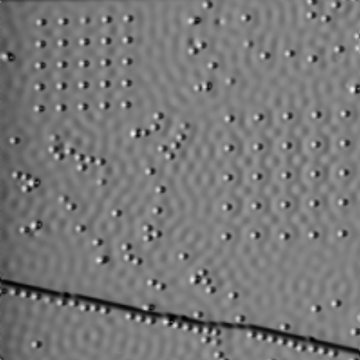
I used the STM to arrange cobalt atoms in the pattern of square lattices on a copper (111) surface. They weren't exactly square since the the sites on the copper (111) surface are arranged in a hexagonal lattice. I also used the STM to image the surface. The STM current is kept constant with a feedback loop and the instrument measures the height of the STM at each point on the surface. By scanning the STM over the entire surface, you get a topographic map of the surface.
Here's a square lattice. The image is a 2D grayscale plot with a light source.
This image is a 3D plot of the STM height with a light source. If you "crash" the STM tip into the surface, you get the "mountain" like features shown in this picture. Sometimes you crash the tip into the surface on purpose in the hope of getting a sharper tip.

The copper surface isn't flat. There are places where the surface is sheared off to a lower atomic layer, resulting in "terraces." You can see a square lattice (the little bumps) on the top lefthand side of the image (also a 3D plot).

No comments:
Post a Comment